- 您现在的位置:买卖IC网 > Sheet目录1223 > KIT35XS3500EVBE (Freescale Semiconductor)KIT EVAL QUAD HIGH SIDE SWITCH
�� �
�
�FUNCTIONAL� DESCRIPTION�
�FUNCTIONAL� PIN� DESCRIPTION�
�CSB�
�SCLK�
�CS�
�SI�
�D15�
�D14�
�D13�
�D12�
�D11�
�D10�
�D9�
�D8�
�D7�
�D6�
�D5�
�D4�
�D3�
�D2�
�D1�
�D0�
�SO�
�OD15� OD14� OD13� OD12� OD11� OD10� OD9�
�OD8�
�OD7�
�OD6�
�OD5�
�OD4�
�OD3�
�OD2�
�OD1� OD0�
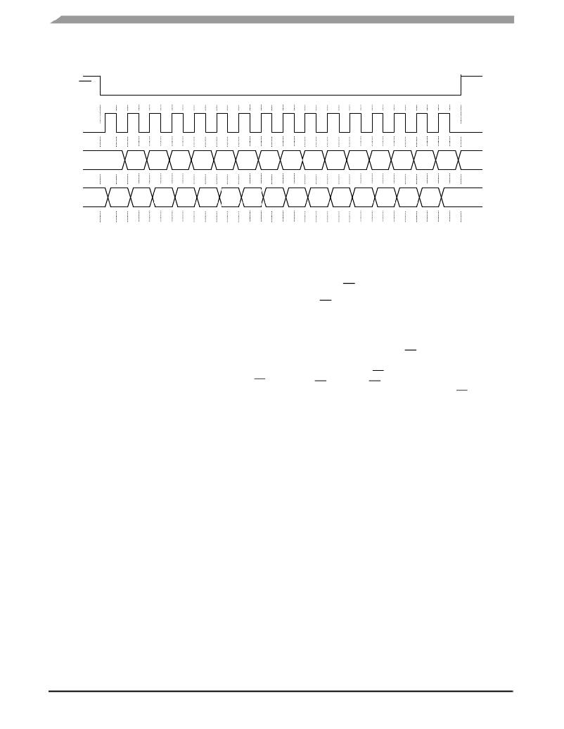
�1.� D15:D0� relate� to� the� most� recent� operation.� entry� of� data� into� the� device.�
�ordered�
�2.� OD15:OD0� and� D15� relate� to� first� most� bits� of� ordered� entry� fault� program� status� into� the� LUX� of� the� device.�
�DO,� D1,� D2,� ...� ,� relate� to� the� the� 16� recent� ordered�
�of� and� data� data� out� IC�
�Notes�
�NOTES:� 1.�
�2.�
�3�
�Serial� Input� (SI)�
�RSTB� is� in� a� logic� H� state� during� the� above�
�device.�
�LUX� IC�
�OD0� OD1� OD2� and� OD15� relate� to� the� first� 16� bits� of� ordered� fault� and� status� data� out� of� the� device.�
�Figure� 8.� Single� 16-Bit� Word� SPI� Communication�
�Chip� Select� (CS)�
�The� SI� pin� is� a� serial� interface� command� data� input� pin.�
�Each� SI� bit� is� read� on� the� falling� edge� of� SCLK.� A� 16-bit�
�stream� of� serial� data� is� required� on� the� SI� pin,� starting� with�
�D15� to� D0.� SI� has� a� passive� pull-down,� R� DOWN� .�
�Serial� Output� (SO)�
�The� SO� data� pin� is� a� tri-state� output� from� the� shift� register.�
�The� SO� pin� remains� in� a� high-impedance� state� until� the� CS�
�pin� is� put� into� a� logic� [0]� state.� The� SO� data� is� capable� of�
�reporting� the� status� of� the� output,� the� device� configuration,�
�and� the� state� of� the� key� inputs.� The� SO� pin� changes� state� on�
�the� rising� edge� of� SCLK� and� reads� out� on� the� falling� edge� of�
�SCLK.�
�The� CS� pin� enables� communication� with� the� master�
�device.� When� this� pin� is� in� a� logic� [0]� state,� the� device� is�
�capable� of� transferring� information� to,� and� receiving�
�information� from,� the� master� device.� The� 35XS3500� device�
�latches� in� data� from� the� Input� Shift� registers� to� the� addressed�
�registers� on� the� rising� edge� of� CS.� The� device� transfers�
�status� information� from� the� power� output� to� the� Shift� register�
�on� the� falling� edge� of� CS.� The� SO� output� driver� is� enabled�
�when� CS� is� logic� [0].� CS� should� transition� from� a� logic� [1]� to� a�
�logic� [0]� state� only� when� SCLK� is� a� logic� [0].� CS� has� a�
�passive� pull-up,� R� UP� .�
�STOP� Input� (STOP)�
�The� STOP� input� wakes� the� device.� It� also� controls� the� Fail�
�mode� activation.� The� signal� is� “high� active“,� meaning� the�
�component� is� active� in� case� of� a� logic� high� at� the� input.�
�35XS3500�
�Analog� Integrated� Circuit� Device� Data� ?�
�22�
�Freescale� Semiconductor�
�发布紧急采购,3分钟左右您将得到回复。
相关PDF资料
KITUSBSPIEVME
KIT EVAL USB-SPI W/MC68HC908JW32
KP3040
KEYPAD USB W/2 USB PORTS
KS8737-EVAL
BOARD EVAL EXPERIMENT FOR KS8737
KSZ8695PX-EVAL
KIT EVAL KSZ8695PX EXPERIMENT
KSZ9692PB-EVAL
BOARD EVALUATION FOR KSZ9692PB
L17-RR-D1-F-01-100
CONN SOCKET 20-24AWG CRIMP GOLD
L171370
D-SUB BACKSHELL BLACK PLAS 9POS
L17529
D-SUB ASSY SPRING LATCH
相关代理商/技术参数
KIT36476
功能描述:电缆组件 1200 in. w/ RJ45 plug and recpt RoHS:否 制造商:Molex 产品:Power Assemblies 类型:Cable Assembly 连接器端口 A:No Connector 连接器端口 A 管脚计数:4 连接器端口 B:No Connector 连接器端口 B 管脚计数: 型式:Male 线规 - 美国线规(AWG):20, 28 长度:0.305 m 颜色:Black, Red
KIT3803MMA7660FC
功能描述:加速传感器开发工具 MMA7660 Eval Kit Daughter Board
RoHS:否 制造商:Murata 工具用于评估:SCA3100-D04 加速:2 g 传感轴:Triple Axis 接口类型:SPI 工作电压:3.3 V
KIT3803MMA7660FC
制造商:Freescale Semiconductor 功能描述:Accelerometer Daughterboard
KIT38073
功能描述:以太网和电信连接器 RJ KIT EMI SHIELDED PANEL MOUNT RoHS:否 制造商:Pulse 产品:Modular Jacks 性能类别: USOC 代码:RJ45 位置/触点数量: 安装风格:Through Hole 端口数量:1 x 1 型式:Female 屏蔽: 电流额定值: 电压额定值: 触点电镀: 外壳材料:Thermoplastic IP 等级:
KIT38081
功能描述:以太网和电信连接器 EMI SHIELD PLUG KIT RoHS:否 制造商:Pulse 产品:Modular Jacks 性能类别: USOC 代码:RJ45 位置/触点数量: 安装风格:Through Hole 端口数量:1 x 1 型式:Female 屏蔽: 电流额定值: 电压额定值: 触点电镀: 外壳材料:Thermoplastic IP 等级:
KIT38081NI
功能描述:以太网和电信连接器 Kit EMI Shield Plug RoHS:否 制造商:Pulse 产品:Modular Jacks 性能类别: USOC 代码:RJ45 位置/触点数量: 安装风格:Through Hole 端口数量:1 x 1 型式:Female 屏蔽: 电流额定值: 电压额定值: 触点电镀: 外壳材料:Thermoplastic IP 等级:
KIT38082
功能描述:以太网和电信连接器 EMI SHIELD RECPT KIT RoHS:否 制造商:Pulse 产品:Modular Jacks 性能类别: USOC 代码:RJ45 位置/触点数量: 安装风格:Through Hole 端口数量:1 x 1 型式:Female 屏蔽: 电流额定值: 电压额定值: 触点电镀: 外壳材料:Thermoplastic IP 等级:
KIT38082NI
功能描述:以太网和电信连接器 RJ KIT EMI SHIELDED RECPT RoHS:否 制造商:Pulse 产品:Modular Jacks 性能类别: USOC 代码:RJ45 位置/触点数量: 安装风格:Through Hole 端口数量:1 x 1 型式:Female 屏蔽: 电流额定值: 电压额定值: 触点电镀: 外壳材料:Thermoplastic IP 等级: